
Torn between monocrystalline and polycrystalline solar panels?
This article offers an in-depth comparison of efficiency, cost, lifespan, and applicable scenarios, along with 2025 buying advice and brand recommendations to help you make an informed decision!
Table of Contents
Solar panel basics
1. How Solar Cells Work
Photovoltaic (PV) power generation, which converts light energy directly into electrical energy, is fundamentally based on the photovoltaic effect. The photovoltaic effect (sometimes also referred to as the photoelectric effect) describes the phenomenon where a semiconductor material generates an electromotive force (voltage) and current when exposed to light.
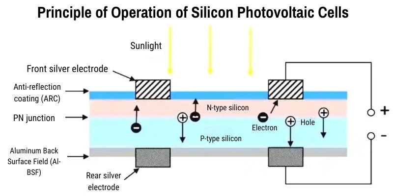
The specific process is as follows: When light shines on the P-N junction of a semiconductor material, the energy of the photons causes the generation of electron-hole pairs within the semiconductor. Under the action of the built-in electric field at the P-N junction, electrons are pushed towards the N-region, and holes are pushed towards the P-region, achieving charge separation. This directional movement and separation of charges creates a voltage between the P-region and the N-region, thereby generating a current. This is the principle of the photovoltaic effect.
2. The Key Role of Silicon Material
I. Silicon Purity and Solar Conversion Efficiency
High-purity silicon material possesses a more perfect crystal structure, which greatly facilitates the migration of charge carriers (electrons and holes) within it, thereby significantly increasing energy conversion efficiency. Simply put, the higher the purity of the silicon material, the stronger the solar panel’s ability to convert solar energy into electrical energy, resulting in higher efficiency. Therefore, in the manufacturing of high-performance solar panels, using high-purity silicon is a core factor in boosting their conversion efficiency.
II. Mainstream Market Silicon Purity Standards
Currently, the silicon purity used in mainstream solar panels on the market (such as multicrystalline and monocrystalline silicon panels) is typically above 99.99%. This level of purity is sufficient to fully meet the requirements of most application scenarios, providing stable, reliable, and efficient power output for residential rooftops, commercial buildings, and large-scale solar power plants alike.
Monocrystalline solar panel
1. Czochralski (CZ) Method Production Process
The Czochralski (CZ) method is one of the dominant processes currently used for producing monocrystalline silicon, holding a significant market share in both the semiconductor and photovoltaic material industries. This process starts with high-purity polycrystalline silicon and involves the precise control of seed crystal introduction and the pulling process to gradually grow monocrystalline silicon ingots that meet industrial standards within a controlled environment. Below are the detailed process steps and key technical aspects:
I. Melting
- High-purity polycrystalline silicon is placed in a quartz crucible and heated above 1414℃ to completely melt and form a silicon melt.
- To prevent impurity contamination, the melting process is conducted in a sealed environment filled with an inert gas, such as argon.
- Strict control over the stability of the quartz crucible is required to minimize oxygen doping, while thermal field design is crucial to ensure uniform melt temperature.
II. Seeding
- A defect-free seed crystal with a specific crystal orientation (e.g., , ) is selected as a template for growth and slowly brought into contact with and immersed in the surface of the silicon melt.
- Precise adjustment of the seed crystal’s rotation speed and immersion depth is critical to prevent crystal cracking caused by sudden temperature changes.
- The seeding process determines the crystal orientation and initial structure of the final monocrystalline silicon ingot, laying the foundation for subsequent growth.
III. Pulling
- After the seed crystal is fully integrated with the silicon melt, the seed crystal is slowly pulled upwards at a constant speed (typically 1-2mm/min) while simultaneously being rotated slowly.
- A dynamic balance between the pulling speed and rotation rate must be maintained to ensure the uniformity and stability of the crystal diameter.
- Real-time monitoring of the crystal diameter (e.g., using a laser diameter measurement system) allows for dynamic adjustments to the pulling speed and furnace temperature, enabling precise control over the crystal shape.
IV. Tail-off
- Once the monocrystalline silicon ingot reaches the target length and diameter, the pulling speed is gradually reduced until it stops, allowing the remaining melt to solidify and complete the crystal growth process.
- The subsequent cooling process also needs to be uniform and stable to minimize internal stress generation within the silicon ingot and prevent the formation of cracks.
2. Core Characteristics
- Uniform monocrystalline structure
- Typical black appearance (or Distinctive black color)
- Distinctive rounded corners (of the cells)
3. Key Advantages
- Higher Efficiency: Achieves high conversion efficiency of 20-25%.
- Stable High-Temperature Performance: Maintains stable and reliable performance output even in high-temperature environments.
- Extended Lifespan: Designed for a lifespan of 25-30 years.
- High Space Utilization: Strong power generation capacity per unit area, making efficient use of installation space.
4. Disadvantages
- Higher production costs, resulting in a relatively high product price.
- High energy consumption during the manufacturing process.
Polycrystalline solar panel
1. Polycrystalline Silicon Production Processes: The Modified Siemens Process Explained
Various methods exist for the production of polycrystalline silicon, primarily including the Modified Siemens Process, Silane Process, Metallurgical Method, Fluidized Bed Reactor Method, Carbothermic Reduction of Silica Method, Electrolysis Method, and Vapor-Liquid Deposition Method, among others. Currently, the Modified Siemens Process dominates the market, accounting for over 80% of global production due to its high process maturity and significant economic benefits, making it the most prevalent industrial production technology. Therefore, this article will focus on detailing this core process.
The Modified Siemens Process is a classic Chemical Vapor Deposition (CVD) process. Its basic principle is as follows: first, high-purity metallurgical silicon (typically requiring purity above 99.5%) is reacted with hydrogen chloride (HCl) to generate trichlorosilane gas (SiHCl₃, referred to as TCS), a key intermediate product that is easy to purify. Subsequently, TCS undergoes deep purification through distillation techniques to remove impurities. Finally, the high-purity TCS gas is introduced into a high-temperature reduction furnace, where it undergoes a reduction reaction and chemical vapor deposition in a hydrogen atmosphere, depositing silicon atoms onto heated silicon rods to grow high-purity polycrystalline silicon ingots. Another important aspect of this process is tail gas treatment and recovery, particularly the dry recovery of unreacted TCS, hydrogen, and silicon tetrachloride (SiCl₄). This achieves a closed-loop recycling of hydrogen and chlorosilanes, enhancing raw material utilization and reducing environmental impact.
The Modified Siemens Process typically comprises the following five main stages:
- SiHCl₃ Synthesis
- SiHCl₃ Distillation and Purification
- SiHCl₃ Hydrogen Reduction and Polysilicon Deposition
- Tail Gas Recovery
- SiCl₄ Hydrogenation and Conversion/Recycling
2. Key Features
- Blue appearance
- Fragmented crystal structure
- Square cells
3. Pros
- Lower manufacturing cost
- Relatively simpler production process
- Higher silicon material utilization, more environmentally friendly
4. Cons
- Relatively lower photoelectric conversion efficiency (typically 15-20%)
- Efficiency degrades faster in high-temperature environments
- Requires larger installation area to achieve the same power output
Key Differences
For easy comparison and understanding, the table below details the key technical parameters of monocrystalline and polycrystalline solar panels.
| Dimension | Monocrystalline Silicon | Polycrystalline Silicon |
|---|---|---|
| Efficiency | 20-25% | 15-20% |
| Cost per Watt | $0.60 | $0.50 |
| Lifespan | 30 years | 25 years |
1. Efficiency and Output
Monocrystalline silicon offers higher photoelectric conversion efficiency, generating more power per unit area. This makes it particularly suitable for roofs or sites with limited installation space.
2. Cost Analysis
Polycrystalline silicon generally has lower manufacturing costs, resulting in a more accessible initial purchase price. While monocrystalline silicon has a higher upfront cost, its greater efficiency and higher long-term power generation can lead to potentially higher long-term returns on investment.
3. Appearance Differences
Aesthetically, monocrystalline silicon cells are typically uniform black with rounded corners, presenting a more sleek appearance. Polycrystalline silicon cells often appear blue or dark blue with straight edges, and their distinct polycrystalline texture has a different impact on visual appeal.
4. Temperature Coefficient
Monocrystalline silicon has a relatively lower temperature coefficient (performance degradation at higher operating temperatures). This means its power generation performance is more stable in hot environments.
5. Applicable Scenarios:
Monocrystalline Silicon: More suitable for projects demanding maximum efficiency, having limited roof or installation area, or where aesthetics are a key consideration.
Polycrystalline Silicon: An option for budget-conscious users with ample installation space who are sensitive to initial costs.
How to Choose: Key Consideration Factors
1. Budget Considerations
Weigh the initial system investment cost against long-term electricity bill savings.
2. Installation Space
For smaller roof areas or situations requiring maximized power generation, higher-efficiency monocrystalline silicon is often preferred; for larger areas, polycrystalline silicon is also a viable option.
3. Geographic Location and Climate
Monocrystalline silicon generally experiences less performance degradation in high-temperature environments, giving it a slight advantage; in moderate climates, both can be considered, and polycrystalline silicon may be more cost-effective.
4. Environmental Factors
The manufacturing process for polycrystalline silicon typically has a lower carbon footprint.
5. Future Expansion and Compatibility
Consider whether the system can be easily upgraded in the future, such as integrating with energy storage systems or other smart devices.
FAQs
Generally, both types have similar design lifespans (typically 25-30 years). However, monocrystalline silicon panels usually exhibit a slower rate of performance degradation compared to polycrystalline panels.
Due to their higher efficiency, monocrystalline silicon panels are relatively more sensitive to partial shading. Shading can lead to a more significant loss in performance. Therefore, in environments with shading, monocrystalline systems often require more careful layout design or the use of technologies like optimizers or microinverters to mitigate the impact. Polycrystalline panels tend to experience slightly less performance loss under partial shading.
It is generally not recommended. Different panel types have varying voltage and current characteristics. Mixing them can lead to reduced overall system efficiency, as the system's performance is often limited by the weakest performing panel. Significant differences could potentially even damage the panels.
Market Trends and Future Outlook
1. Technology Iteration Directions
With the maturation and widespread adoption of high-efficiency technologies such as PERC and TOPCon, monocrystalline silicon has become the market mainstream, with its efficiency continuously increasing, while the market share of polycrystalline silicon shows a declining trend.
2. Impact of Emerging Technologies
Regarding emerging technologies like thin-film solar and perovskites, their future development and whether they have the potential to replace traditional silicon-based photovoltaic products remain key areas of focus for the industry.
Conclusion
Known for high efficiency and a compact footprint, monocrystalline silicon solar panels are commonly applied in solar lighting products. For solar lighting professionals, selecting these panels as components is a top choice.
Polycrystalline silicon panels are more affordable and suited for budget-sensitive applications, like rooftop energy storage systems, where they are often the go-to option.
Nevertheless, with sufficient budget, opting for monocrystalline silicon panels is advisable for superior long-term performance and higher efficiency, better meeting future energy needs.